Master PCB Design Build Real Circuit Boards
From schematic capture to manufactured boards. Learn KiCad, routing rules, Gerber files, and professional manufacturing — design your first PCB with confidence.
📋 Course Overview
This comprehensive course takes you from complete beginner to confident PCB designer. Each module builds on the previous, with interactive calculators, real-world examples, and video tutorials to reinforce learning.
What is a PCB?
History, types, and anatomy of printed circuit boards
PCB Materials
FR-4, copper weights, solder mask & silkscreen layers
Schematic Capture
Circuit design, symbols, nets & ERC checking
Component Library
Symbols, footprints, 3D models & library management
Footprints & Pads
Through-hole, SMD pads, land patterns & thermal pads
Board Setup
Board outline, layer stack, rules & constraints
Trace Routing
Routing strategies, differential pairs & impedance control
Ground & Power
Power planes, copper pours, decoupling & thermal management
Multi-Layer PCBs
Layer stackup, vias, blind/buried vias & HDI
Design Rules (DRC)
Clearance, trace width, annular rings & manufacturing limits
EMC & Signal Integrity
Crosstalk, return paths, shielding & noise reduction
Gerber & Fabrication
Gerber output, drill files, BOM & ordering from JLCPCB
Soldering & Assembly
Hand soldering, reflow, stencils & pick-and-place
PCB Calculator
Trace width, via current & impedance calculators
Final Quiz
25 questions to test your PCB design knowledge
🧰 Software & Tools You'll Need
KiCad 8
Free, open-source EDA suite for schematic & layout
Computer
Any modern PC or Mac — KiCad runs on all platforms
Calipers
Digital calipers for measuring component dimensions
Soldering Iron
Temperature-controlled station for board assembly
Magnifier
Magnifying glass or USB microscope for inspection
JLCPCB Account
Free account to order your manufactured boards
What is a PCB?
Discover the backbone of every electronic device — the Printed Circuit Board — its history, types, and fundamental anatomy.
🔧 Introduction to PCBs
A Printed Circuit Board (PCB) is a flat board made of insulating material with conductive copper pathways etched or printed onto it. These copper pathways — called traces — connect electronic components together, replacing the need for messy point-to-point wiring.
PCBs are found in virtually every electronic device: your smartphone, laptop, TV, car dashboard, medical equipment, satellites, and even humble LED flashlights. They are the foundation of modern electronics manufacturing.
📜 A Brief History
Before PCBs, electronic circuits were built using point-to-point wiring — each component was connected with individual wires soldered directly. This was slow, error-prone, and unreliable.
- 1936 — Paul Eisler created the first PCB while working on a radio in England
- 1943 — The US military adopted PCB technology for proximity fuses in WWII
- 1950s — Through-hole technology became standard for manufacturing
- 1960s — Double-sided PCBs and plated through-holes revolutionized density
- 1980s — Surface Mount Technology (SMT) enabled much smaller components
- 2000s — HDI (High Density Interconnect) boards with micro-vias emerged
- Today — 20+ layer boards with 50µm features are routine in smartphones
🗂️ Types of PCBs
| Type | Layers | Complexity | Common Use |
|---|---|---|---|
| Single-Sided | 1 copper layer | Low | Simple toys, LEDs, calculators |
| Double-Sided | 2 copper layers | Medium | Arduino shields, power supplies |
| Multi-Layer | 4, 6, 8+ layers | High | Computers, smartphones, servers |
| Rigid | Any | Varies | Most electronics |
| Flexible | 1-4 layers | High | Wearables, camera modules |
| Rigid-Flex | 4-10+ layers | Very High | Smartphones, aerospace |
| Metal-Core (MCPCB) | 1-2 layers | Medium | High-power LEDs, motor drivers |
🔍 Anatomy of a PCB
A typical PCB consists of several key layers:
- Substrate (FR-4) — The fiberglass-reinforced epoxy base material that provides structural strength
- Copper Layers — Thin copper foil (typically 1oz = 35µm thick) where the circuit traces are etched
- Solder Mask — The green (or other color) coating that protects copper from oxidation and prevents solder bridges
- Silkscreen — White printed text showing component labels, reference designators, and logos
- Surface Finish — A protective coating on exposed pads (HASL, ENIG, OSP) to ensure solderability
The reason most PCBs are green is because the solder mask was traditionally green — it provided the best contrast for visual inspection. Today you can order PCBs in virtually any color: black, white, red, blue, purple, and even transparent!
🎥 Video: What is a PCB?

PCB Materials & Layers
Understand the materials that make up a PCB — from the substrate to the surface finish — and how each layer serves a critical function.
🧱 Substrate Materials
The substrate is the base material of the PCB that provides mechanical support and electrical insulation between copper layers.
| Material | Tg (°C) | Dk | Cost | Use Case |
|---|---|---|---|---|
| FR-4 Standard | 130-140 | 4.5 | Low | General purpose, hobby, most products |
| FR-4 High-Tg | 170-180 | 4.5 | Medium | Lead-free assembly, automotive |
| Rogers | 280+ | 2.2-10.2 | High | RF/microwave, antennas, high-speed |
| Aluminum (MCPCB) | N/A | N/A | Medium | LED lighting, power electronics |
| Polyimide (Flex) | 250+ | 3.5 | High | Flexible circuits, wearables |
| Ceramic (LTCC) | N/A | 5-10 | Very High | Military, aerospace, high-reliability |
Glass Transition Temperature (Tg) is the temperature at which the substrate softens. For lead-free soldering (peak ~260°C), use High-Tg FR-4. Standard FR-4 is fine for leaded solder (~220°C peak).
🥉 Copper Weight & Thickness
Copper thickness is specified in ounces per square foot (oz/ft²). This tells you how thick the copper foil is on each layer.
| Copper Weight | Thickness (µm) | Thickness (mils) | Typical Use |
|---|---|---|---|
| 0.5 oz | 17.5 | 0.7 | Fine-pitch, high-density inner layers |
| 1 oz (standard) | 35 | 1.4 | General purpose — most common |
| 2 oz | 70 | 2.8 | Power traces, high current |
| 3 oz | 105 | 4.2 | Heavy power, motor drives |
🟢 Solder Mask
The solder mask is a protective lacquer coating applied over the copper traces. It serves several crucial functions:
- Prevents oxidation of copper traces
- Prevents solder bridges between pads during assembly
- Provides electrical insulation between traces
- Protects against dust, moisture, and contamination
Available colors: Green (classic), Black, White, Red, Blue, Yellow, Purple, Matte Black, Matte Green.
✍️ Silkscreen
The silkscreen layer contains printed text and symbols for component identification. Best practices:
- Minimum text height: 0.8mm (1mm recommended)
- Minimum line width: 0.15mm
- Include reference designators (R1, C2, U3) next to components
- Add polarity marks for diodes, electrolytic caps, and ICs
- Include pin-1 indicators, test points, and board version numbers
✨ Surface Finish
| Finish | Shelf Life | Flatness | Lead-Free? | Cost |
|---|---|---|---|---|
| HASL (Hot Air Solder Leveling) | 12+ months | Poor | Leaded available | Low |
| Lead-Free HASL | 12+ months | Poor | Yes | Low-Med |
| ENIG (Immersion Gold) | 12+ months | Excellent | Yes | Medium |
| OSP (Organic) | 6 months | Excellent | Yes | Lowest |
| Immersion Tin | 6 months | Excellent | Yes | Medium |
| Hard Gold | Years | Excellent | Yes | Highest |
For hobby projects, HASL is cheapest and most forgiving for hand soldering. For fine-pitch SMD (QFP, BGA), use ENIG for flat pads. For connectors that need repeated insertion, use Hard Gold.
🎥 Video: PCB Manufacturing Process

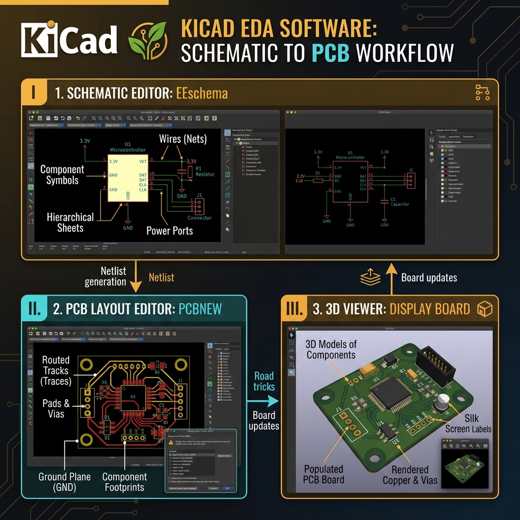
Schematic Capture
Learn to create professional circuit schematics — the blueprint for your PCB design — using KiCad's schematic editor.
📝 What is a Schematic?
A schematic is a symbolic diagram of an electronic circuit. Unlike a physical layout, a schematic shows the logical connections between components without representing their physical placement. It is the first step in any PCB design process.
Think of a schematic as the architectural blueprint — it defines what's connected to what. The PCB layout is the construction plan — it defines where everything physically goes.
🔣 Schematic Symbols
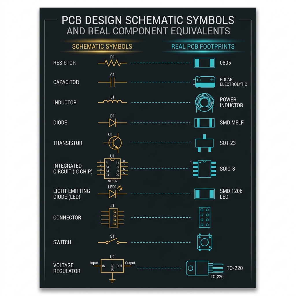
Standard schematic symbols you need to know:
| Component | Symbol | Designator | Example |
|---|---|---|---|
| Resistor | Zigzag / Rectangle | R1, R2... | R1 = 10kΩ |
| Capacitor | Two parallel lines | C1, C2... | C1 = 100nF |
| Inductor | Coil / Bumps | L1, L2... | L1 = 10µH |
| Diode | Triangle + Bar | D1, D2... | D1 = 1N4148 |
| LED | Diode + Arrows | D3, LED1... | LED1 = Green |
| Transistor (NPN) | Three terminal symbol | Q1, Q2... | Q1 = 2N2222 |
| MOSFET | Gate-arrowed symbol | Q3, M1... | M1 = IRLZ44N |
| IC / Microcontroller | Rectangle with pins | U1, U2... | U1 = ATmega328P |
| Connector | Pins in a row | J1, J2... | J1 = USB-C |
| Power Symbols | VCC ▲, GND ▼ | — | +3.3V, +5V, GND |
🌐 Nets & Connections
In a schematic, connections are represented by wires (nets). When two wires cross, they are NOT connected unless there is a junction dot. Key concepts:
- Net — A named electrical connection (e.g., VCC, GND, SDA, SCK)
- Net Label — A text tag placed on a wire to name the connection without drawing a physical wire
- Power Flag — Tells the ERC that a net is intentionally powered
- No-Connect (X) — Marks unused pins so the ERC doesn't flag them as errors
- Junction Dot — Connects crossing wires; without it, wires just pass over each other
✅ Electrical Rules Check (ERC)
The ERC is an automated check that catches common schematic mistakes:
- Unconnected pins — Pins that should be connected but aren't
- Power conflicts — Two outputs driving the same net
- Missing power flags — Power nets without a defined source
- Short circuits — Direct connections between power and ground
Always run the ERC before proceeding to PCB layout. Fixing mistakes in the schematic is 100× cheaper than fixing them on a manufactured board!
⌨️ KiCad Schematic Shortcuts
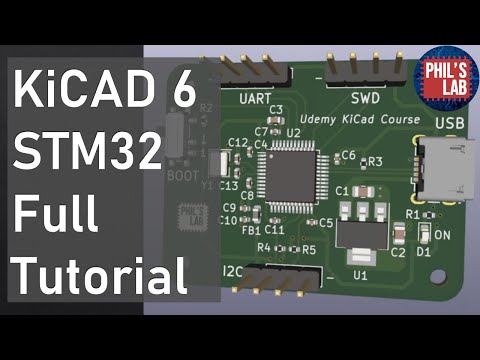
🎥 Video: KiCad Schematic Tutorial
Open KiCad and create a simple schematic with an LED, a 330Ω resistor, and a 2-pin connector. Connect them in series and add VCC/GND power symbols. Run the ERC and fix any errors.
Component Libraries
Master the art of managing symbols, footprints, and 3D models — the building blocks of every schematic and PCB layout.
📚 Library Structure
In KiCad, every component needs three things:
- Schematic Symbol — The visual representation in the circuit diagram (e.g., a resistor zigzag)
- PCB Footprint — The physical copper pattern on the board where the component is soldered
- 3D Model (optional) — A STEP/WRL file for visual verification and mechanical clearance checks
KiCad comes with extensive built-in libraries, but for professional work you'll often need to create custom libraries or download from manufacturers.
🔍 Finding Components
Best sources for component data:
Manufacturer Sites
TI, STM, Microchip provide official KiCad/Altium libraries
SnapEDA
Free symbols, footprints & 3D models for thousands of parts
Ultra Librarian
CAD models from major distributors like Mouser & DigiKey
Component Search Engine
Search across 15+ EDA formats at componentsearchengine.com
KiCad Built-in
Thousands of common parts included with KiCad installation
Custom Creation
Build your own using KiCad's symbol and footprint editors
🏷️ Reference Designators
| Prefix | Component Type | Example |
|---|---|---|
| R | Resistor | R1, R2, R15 |
| C | Capacitor | C1, C2, C10 |
| L | Inductor | L1, L2 |
| D | Diode / LED | D1, D2 |
| Q | Transistor (BJT/MOSFET) | Q1, Q2 |
| U | IC / Microcontroller | U1, U2 |
| J | Connector | J1, J2 |
| SW | Switch | SW1, SW2 |
| F | Fuse | F1 |
| Y | Crystal / Oscillator | Y1 |
| TP | Test Point | TP1, TP2 |
| FB | Ferrite Bead | FB1, FB2 |
📋 Bill of Materials (BOM)
The BOM is a spreadsheet listing every component needed to build the board. A good BOM includes:
- Reference Designator — R1, C2, U3
- Value — 10kΩ, 100nF, LM7805
- Footprint — 0805, SOT-23, SOIC-8
- Manufacturer Part Number (MPN) — e.g., RC0805FR-0710KL
- Supplier & SKU — LCSC C17414, DigiKey 311-10KARCT-ND
- Quantity — How many of each part per board
Always include the MPN (Manufacturer Part Number) in your BOM. Generic values like "10kΩ" are ambiguous — there are hundreds of 10kΩ resistors. The MPN uniquely identifies the exact part.
🎥 Video: Creating Custom Libraries

Footprints & Pads
Understand the physical copper patterns that components solder to — the bridge between your schematic and the real board.
👣 What is a Footprint?
A footprint (also called a land pattern) is the copper pad pattern on the PCB where a component is physically soldered. Every component in your schematic must be assigned a matching footprint.
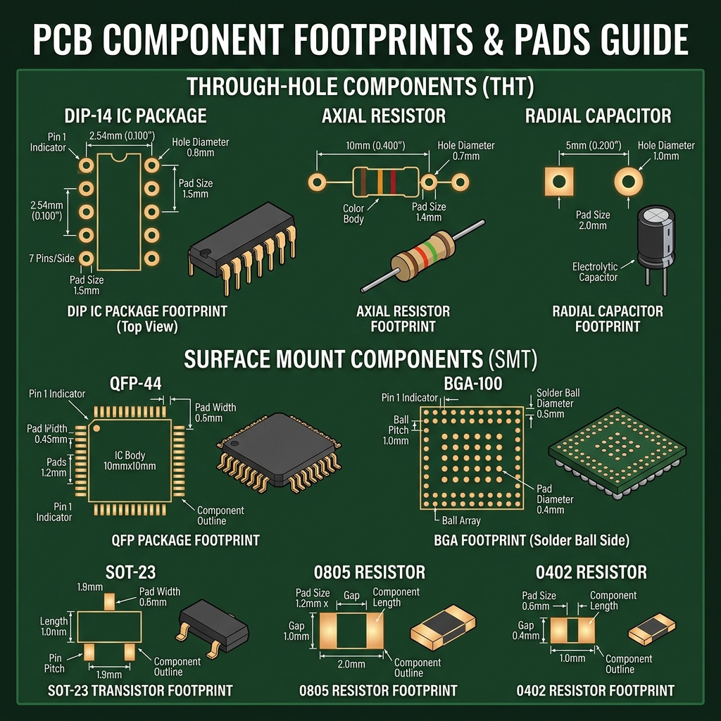
🔌 Through-Hole (THT) Pads
Through-hole pads have a drilled hole that the component lead passes through and is soldered on the opposite side.
| Parameter | Typical Value | Notes |
|---|---|---|
| Drill Diameter | Lead diameter + 0.2-0.3mm | Allows easy insertion |
| Pad Diameter | Drill + 0.5mm minimum | Annular ring requirement |
| Annular Ring | ≥0.15mm (fab minimum) | 0.25mm recommended |
The annular ring is the copper that surrounds the drill hole. It must be large enough for reliable soldering. Most fabs require minimum 0.15mm, but 0.25mm is safer — especially for beginners.
📏 SMD Pad Sizes
Surface Mount Device (SMD) pads sit flat on the board surface. Common passive component sizes:
| Package | Size (mm) | Size (mils) | Hand Solderable? |
|---|---|---|---|
| 0805 | 2.0 × 1.25 | 80 × 50 | Easy ✅ |
| 0603 | 1.6 × 0.8 | 60 × 30 | Moderate ✅ |
| 0402 | 1.0 × 0.5 | 40 × 20 | Difficult ⚠️ |
| 0201 | 0.6 × 0.3 | 24 × 12 | Microscope needed ❌ |
| 01005 | 0.4 × 0.2 | 16 × 8 | Machine only ❌ |
🔥 Thermal Pads
Many power ICs and voltage regulators have a exposed thermal pad on the bottom. This pad must be connected to a large copper pour (usually ground) with multiple thermal vias to dissipate heat.
- Use a grid of 0.3mm vias spaced 1mm apart under the pad
- Connect to an inner ground plane for maximum heat spreading
- Apply solder paste at 50-80% of the pad area (too much causes the IC to float during reflow)
🎥 Video: SMD vs Through-Hole
Board Setup
Configure your PCB project — define the board outline, layer stackup, design rules, and constraints before placing a single component.
📐 Board Outline
The board outline (Edge.Cuts layer in KiCad) defines the physical boundary of your PCB. Best practices:
- Use round corners (radius ≥ 0.5mm) — sharp corners create stress concentrations
- Keep components at least 1mm from the board edge
- Standard board thickness: 1.6mm (most common), 0.8mm, 1.0mm also available
- Consider mounting holes — M3 (3.2mm drill) is standard
- For enclosures, check mechanical clearance with the 3D viewer
📊 Design Rule Setup
Before routing, configure your Design Rules based on your manufacturer's capabilities:
| Parameter | JLCPCB Standard | JLCPCB Advanced | Professional |
|---|---|---|---|
| Min Trace Width | 0.127mm (5mil) | 0.09mm (3.5mil) | 0.075mm (3mil) |
| Min Clearance | 0.127mm (5mil) | 0.09mm (3.5mil) | 0.075mm (3mil) |
| Min Via Drill | 0.3mm | 0.2mm | 0.1mm (laser) |
| Min Via Diameter | 0.6mm | 0.45mm | 0.25mm |
| Min Annular Ring | 0.13mm | 0.1mm | 0.075mm |
| Min Hole Size | 0.3mm | 0.15mm | 0.1mm |
Always check your fab's capabilities page before designing. Using dimensions below their minimums will cause your order to be rejected or manufactured incorrectly. When in doubt, use bigger values!
🎥 Video: KiCad PCB Layout Setup
Trace Routing
The art and science of copper trace routing — learn strategies, best practices, and professional techniques for reliable connections.
🛤️ Routing Fundamentals
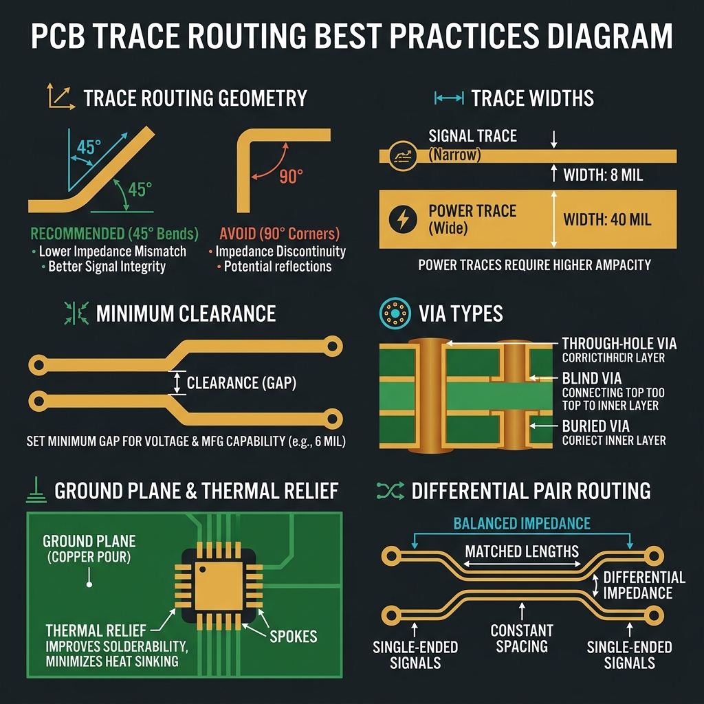
Routing is the process of drawing copper traces to connect component pads according to the netlist from your schematic. Key principles:
- Route signals first, then power, then ground (or use planes for power/ground)
- Use 45° angles — never 90° corners (they create impedance discontinuities and acid traps)
- Keep traces as short as possible — shorter traces = less resistance, less EMI
- Avoid running traces parallel for long distances — this causes crosstalk
- Use wider traces for power (25-50 mil) and normal width for signals (8-10 mil)
📏 Trace Width vs Current
The trace must be wide enough to carry the required current without excessive heating. The standard reference is IPC-2221:
| Current (A) | 1oz External (mils) | 1oz Internal (mils) | 2oz External (mils) |
|---|---|---|---|
| 0.5A | 10 | 20 | 5 |
| 1.0A | 20 | 40 | 10 |
| 2.0A | 45 | 90 | 22 |
| 3.0A | 80 | 150 | 35 |
| 5.0A | 150 | 300 | 70 |
For a 10°C temperature rise on external 1oz copper: Width (mils) ≈ Current² × 25. Use the calculator in Module 14 for precise values!
🔀 Differential Pairs
Differential pairs are two traces that carry complementary signals (USB, Ethernet, HDMI). They must be routed with:
- Matched length — Both traces must be the same length (within 0.1mm)
- Consistent spacing — Fixed gap between the two traces
- Controlled impedance — Usually 90Ω differential (USB) or 100Ω (Ethernet)
- Symmetrical routing — Route both traces together, never split them
⌨️ KiCad Routing Shortcuts
🎥 Video: PCB Routing Techniques

Ground & Power Design
Master power distribution — from ground planes and copper pours to decoupling strategies and thermal management.
⚡ Ground Plane
A ground plane is a large copper pour connected to GND that covers most of a layer. It's arguably the single most important design technique in PCB design:
- Low impedance return path — Provides the shortest path for return currents
- EMI reduction — Acts as a shield against electromagnetic interference
- Thermal management — Spreads heat across the board
- Simplifies routing — No need to route individual GND traces
Avoid cutting slots or gaps in your ground plane. Slots force return currents to take long detours, creating antenna-like loops that radiate EMI. If analog and digital sections exist, use a single ground plane with components separated by region.
🔋 Power Distribution
Power traces need special attention because they carry the most current:
- Use wide traces (30-50 mil minimum) or dedicated power planes
- Place bulk capacitors (10-100µF electrolytic) near the power input
- Place decoupling capacitors (100nF ceramic) within 3mm of each IC's VCC pin
- Consider a star-point grounding topology for mixed-signal boards
🧊 Decoupling Best Practices
Every IC needs decoupling capacitors close to its power pins to filter high-frequency noise:
100nF ceramic capacitor
Place within 3mm of each VCC pin. This handles mid-frequency noise (1-100 MHz). One per power pin minimum.
10µF bulk capacitor
Place near each power regulator output. Handles low-frequency ripple and provides local charge reservoir.
1nF – 10nF for high-speed
For high-speed ICs (>100 MHz), add another smaller cap for very high frequency decoupling.
Route: IC → cap → via → plane
The current path should go from IC VCC pin → capacitor → via to power plane. Keep this path as short as possible.
🔥 Thermal Management
Components that dissipate significant power need thermal design consideration:
- Use thermal vias under thermal pads — multiple 0.3mm vias in a grid pattern
- Connect to large copper pours on inner and outer layers for heat spreading
- Use thermal relief on pads connected to planes (flower pattern with spokes) for easier soldering
- Consider heatsinks or forced airflow for high-power designs
🎥 Video: Power Integrity

Multi-Layer PCBs
Go beyond 2 layers — learn layer stackup design, via types, and when to use 4-layer or 6-layer boards.
📚 Why Multi-Layer?
As designs grow in complexity, two layers aren't enough. Multi-layer boards provide:
- Dedicated power and ground planes — Improved power distribution and EMC
- More routing channels — Complex ICs with 100+ pins need the space
- Controlled impedance — Consistent trace impedance for high-speed signals
- Smaller board size — More routing layers = denser component placement
🏗️ 4-Layer Stackup
The most common multi-layer configuration. The standard 4-layer stackup is:
| Layer | Type | Function |
|---|---|---|
| Layer 1 (Top) | Signal + Components | Component side routing |
| Layer 2 (Inner 1) | Ground Plane | Continuous ground reference |
| Layer 3 (Inner 2) | Power Plane | VCC, 3.3V, 5V distribution |
| Layer 4 (Bottom) | Signal + Components | Bottom side routing |
Signal-Ground-Power-Signal gives the best EMC performance. The ground plane is adjacent to both signal layers, providing a close return path. The tight coupling between signal and ground plane also gives controlled impedance.
🕳️ Via Types
| Via Type | Description | Cost | When to Use |
|---|---|---|---|
| Through-Hole Via | Drills through all layers | Standard ✅ | Most connections — cheapest option |
| Blind Via | Connects surface to inner layer | Expensive | BGA fanout on outer layers |
| Buried Via | Connects two inner layers | Very Expensive | HDI designs, complex routing |
| Micro Via | Laser-drilled, tiny diameter | Very Expensive | Fine-pitch BGA, smartphones |
🎥 Video: Multi-Layer PCB Design
Design Rules & DRC
Learn the manufacturing constraints every PCB designer must follow — and how the Design Rule Check ensures your board can be built.
📏 Critical Design Rules
Design rules ensure your PCB can be manufactured reliably. The three most critical parameters:
- Minimum Trace Width — The narrowest copper path allowed (typically 5-6 mil / 0.127-0.15mm)
- Minimum Clearance — The smallest gap between copper features (typically 5-6 mil)
- Minimum Drill Size — The smallest hole the fab can drill (typically 0.3mm mechanical, 0.1mm laser)
🔍 Common DRC Errors
Clearance Violation
Copper features too close — will cause short circuits
Unconnected Net
Ratsnest line remaining — missing trace or via connection
Annular Ring Too Small
Insufficient copper around drill hole — may break during manufacturing
Trace Width Violation
Trace narrower than minimum — may be etched away in manufacturing
Copper in Courtyard
Traces underneath component — potential assembly issue
Minimum Hole Size
Drill too small for the fab's capability — order rejection
✅ Running the DRC
In KiCad, run Inspect → Design Rules Check (or click the ladybug icon). The DRC will flag:
- Errors (red) — Must be fixed. Board won't work correctly.
- Warnings (yellow) — Should be reviewed. May or may not be problems.
- Exclusions — Items you've manually marked as acceptable.
Your design should have ZERO DRC errors before generating Gerber files. Warnings should be individually reviewed and either fixed or intentionally excluded with a documented reason.
🎥 Video: DRC Deep Dive

EMC & Signal Integrity
Understand how PCB layout affects electromagnetic compatibility and signal quality — from crosstalk to impedance matching.
📡 What is EMC?
Electromagnetic Compatibility (EMC) is the ability of your circuit board to:
- Not emit excessive electromagnetic interference (EMI) to other devices
- Not be susceptible to external interference from other sources
Poor PCB layout is the #1 cause of EMC failures. Even a perfectly designed circuit can fail EMC testing if the PCB layout creates unintended antenna structures.
🔊 Crosstalk
Crosstalk occurs when a signal on one trace induces noise on an adjacent trace via capacitive or inductive coupling:
- Keep parallel runs short — Maximum 1-2 inches of parallel traces
- Increase spacing — The "3W rule": center-to-center spacing ≥ 3× trace width
- Use ground guards — Place grounded traces between sensitive signal pairs
- Route on different layers — Perpendicular crossing minimizes coupling
🔄 Return Path
Every signal has a return current that flows back to the source. This return current follows the path of least impedance — at high frequencies, that's directly underneath the signal trace on the ground plane.
Never route high-speed signals over gaps or splits in the ground plane. The return current has no path and will take a long detour, creating a large current loop that radiates EMI like an antenna.
📐 Impedance Control
High-speed signals require controlled impedance — the trace geometry must produce a specific impedance value:
| Interface | Impedance | Type |
|---|---|---|
| USB 2.0 | 90Ω differential | Differential pair |
| USB 3.0/3.1 | 90Ω differential | Differential pair |
| HDMI | 100Ω differential | Differential pair |
| Ethernet (100/1000) | 100Ω differential | Differential pair |
| DDR4 Memory | 40Ω single-ended | Single-ended |
| PCIe | 85Ω differential | Differential pair |
| General digital | 50Ω single-ended | Single/Microstrip |
🛡️ EMC Design Checklist
- ✅ Continuous ground plane with no splits or slots under signal traces
- ✅ Decoupling capacitors (100nF) on every IC power pin within 3mm
- ✅ Short, wide power traces or power planes
- ✅ 45° routing angles, no 90° corners
- ✅ Avoid routing under crystals or oscillators
- ✅ Keep high-speed signals away from board edges
- ✅ Use differential pairs for high-speed interfaces
- ✅ Place decoupling caps on the same layer as the IC
- ✅ Ground via stitching around board perimeter
- ✅ Separate analog and digital sections physically
🎥 Video: EMC for PCB Designers

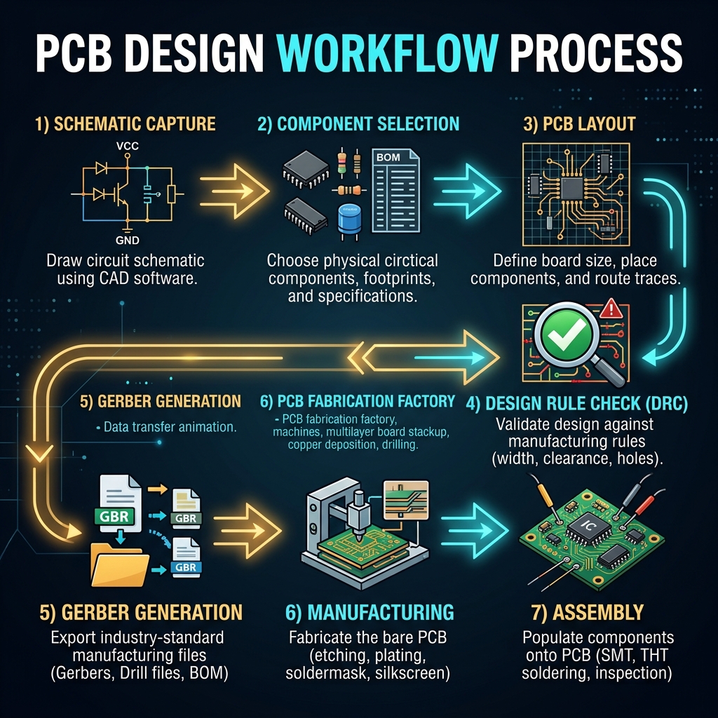
Gerber Files & Fabrication
Export your design for manufacturing — generate Gerber files, drill files, and order your first board from JLCPCB or PCBWay.
📁 What are Gerber Files?
Gerber files are the industry standard file format for PCB manufacturing. Each file represents one layer of your board:
| File | Extension | Content |
|---|---|---|
| Top Copper | .gtl / F.Cu.gbr | Front copper traces and pads |
| Bottom Copper | .gbl / B.Cu.gbr | Back copper traces and pads |
| Top Solder Mask | .gts / F.Mask.gbr | Front solder mask openings |
| Bottom Solder Mask | .gbs / B.Mask.gbr | Back solder mask openings |
| Top Silkscreen | .gto / F.Silkscreen.gbr | Front text and labels |
| Bottom Silkscreen | .gbo / B.Silkscreen.gbr | Back text and labels |
| Board Outline | .gm1 / Edge.Cuts.gbr | PCB shape / cut boundary |
| Drill File | .drl / .xln | Through-hole and via drill data |
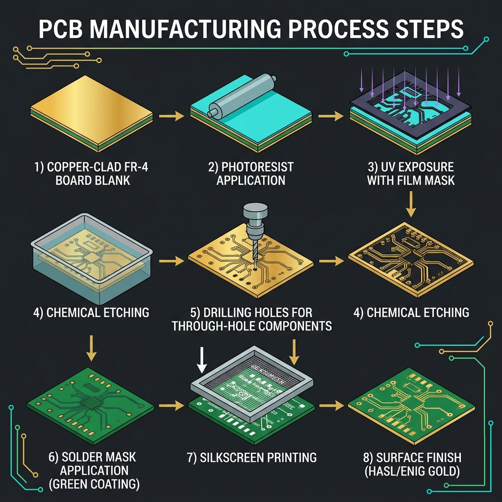
📤 Exporting from KiCad
Run DRC first
Inspect → Design Rules Check. Ensure zero errors before exporting.
Generate Gerbers
File → Fabrication Outputs → Gerbers (.gbr). Select all required layers, use origin "Drill/Place file origin".
Generate Drill File
In the Gerber dialog, click "Generate Drill Files". Use Excellon format, metric units, PTH and NPTH in separate files.
Verify in Gerber Viewer
Open KiCad's GerbView or use an online viewer (gerber-viewer.ucamco.com) to inspect all layers.
ZIP and Upload
Put all .gbr and .drl files in a ZIP archive and upload to your chosen fab.
🏭 PCB Manufacturing Process
🛒 Popular PCB Fabs & Pricing
| Fabricator | Min Order | 2-Layer Price | Lead Time | Assembly? |
|---|---|---|---|---|
| JLCPCB | 5 pcs | $2-5 | 2-7 days | Yes (SMT) |
| PCBWay | 5 pcs | $5-10 | 3-7 days | Yes (THT+SMT) |
| OSH Park | 3 pcs | $5/in² | 7-14 days | No |
| Aisler | 3 pcs | €8-15 | 5-10 days | Yes (SMT) |
| AllPCB | 5 pcs | $1-5 | 2-5 days | Yes |
JLCPCB offers the best combination of price and quality for hobby and prototype boards. Their standard 2-layer boards (≤100×100mm) start at ~$2 for 5 boards. Combine with their SMT assembly service for fully assembled boards.
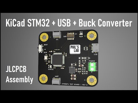
🎥 Video: Ordering from JLCPCB

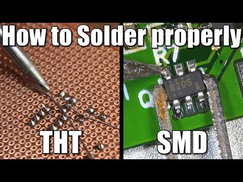
Soldering & Assembly
Learn the techniques to populate your manufactured PCB — from hand soldering to reflow ovens and pick-and-place machines.
🔧 Hand Soldering Basics
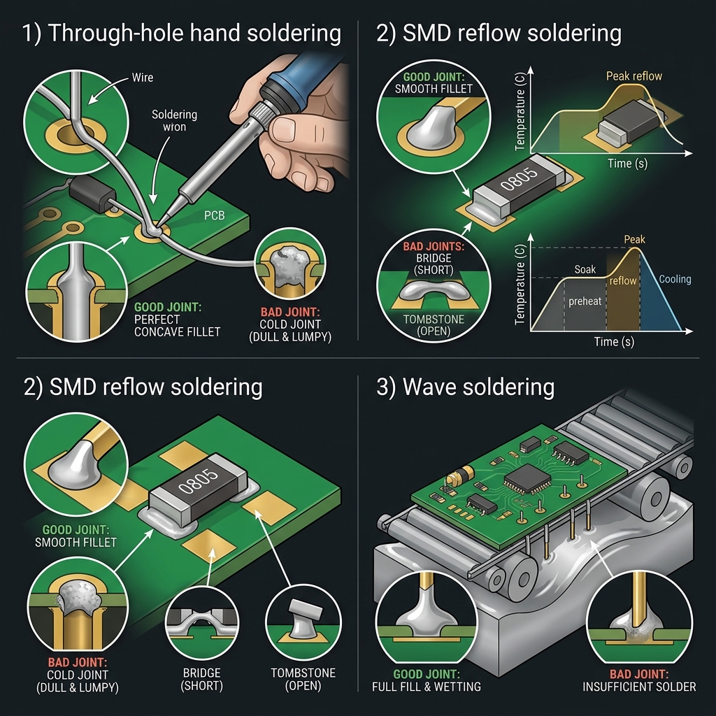
For hobby and prototype boards, hand soldering is the most common method:
Clean the tip
Tin the soldering iron tip with a small amount of solder. Use a brass sponge to clean excess.
Heat the joint
Touch the iron to both the pad AND the component lead simultaneously. Heat for 1-2 seconds.
Apply solder
Feed solder wire to the joint (not the iron). The solder should flow and wick onto both surfaces.
Remove solder, then iron
Remove the solder wire first, then the iron. Hold the component still until the joint solidifies.
✅ Good vs Bad Solder Joints
| Quality | Appearance | Cause |
|---|---|---|
| Perfect ✅ | Shiny, concave fillet, smooth | Proper temperature and timing |
| Cold Joint ❌ | Dull, grainy, rough surface | Insufficient heat or movement during cooling |
| Too Much Solder ❌ | Blobby, convex dome | Excessive solder applied |
| Bridge ❌ | Solder shorts between pads | Too much solder on fine-pitch pins |
| Tombstone ❌ | SMD component stands upright | Uneven heating during reflow |
| Dry Joint ❌ | No solder fillet visible | Pad or lead not hot enough |
🔥 SMD Soldering Techniques
- Drag Soldering — For fine-pitch ICs (QFP): tin one corner pad, align IC, solder remaining pins by dragging solder across all pins, wick excess with solder wick
- Hot Air Rework — Apply solder paste, place components, use hot air station (350-380°C) to reflow
- Solder Paste + Toaster Oven — DIY reflow: apply paste with stencil, place components, reflow in modified toaster oven with temperature control
- Hot Plate — Similar to toaster oven but using a ceramic hot plate (~220-250°C)
🏭 Professional Assembly (PCBA)
For production quantities, use a PCB Assembly (PCBA) service:
- Solder Paste Stencil — Laser-cut stainless steel stencil applies precise solder paste
- Pick and Place — Robotic machine places components at high speed (20,000+ CPH)
- Reflow Oven — Controlled temperature profile melts solder paste (preheat → soak → reflow → cool)
- AOI (Automated Optical Inspection) — Camera system checks for missing/misaligned components
- Wave Soldering — For through-hole components after SMD reflow
🎥 Video: SMD Soldering Masterclass

PCB Calculator
Interactive tools to calculate trace width, via current capacity, and microstrip impedance for your designs.
📏 Trace Width Calculator (IPC-2221)
Calculate the minimum trace width for a given current, based on IPC-2221 standard.
🕳️ Via Current Calculator
Estimate the current-carrying capacity of a via based on its dimensions.
📐 Microstrip Impedance Calculator
Calculate the characteristic impedance of a microstrip trace over a ground plane.
🔄 Unit Converter
1 mil = 0.0254 mm | 1 mm = 39.37 mils
PCB Design Final Quiz
Test your knowledge with 25 questions covering everything from materials to manufacturing. Score 80% or higher to earn your certificate!

PCB Design Masterclass — From Zero to Professional Board